You will find the design file for the updated test board here.
The first drawing in the design file has some remarks on board production
which may be useful.
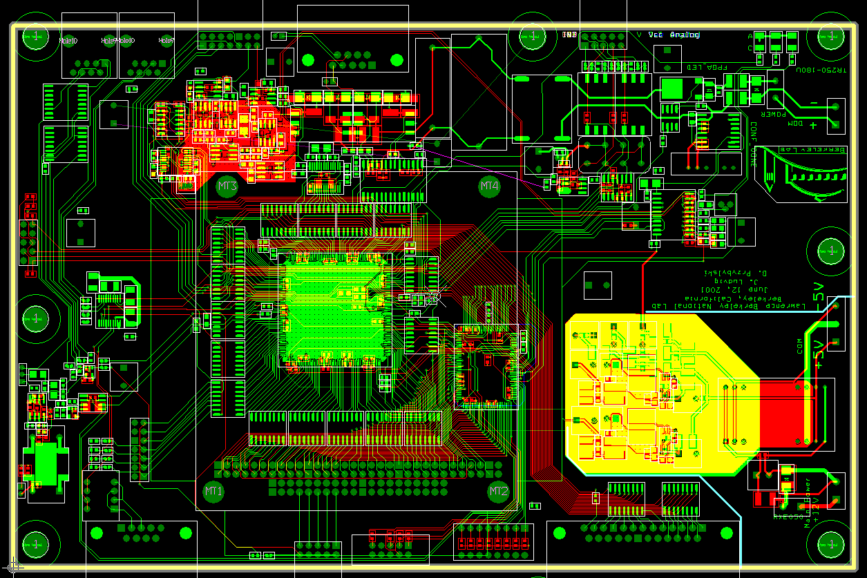
You will find a layout for the updated test board here.
(see below)
The layout shows 100% routed, but is not 'cleaned up'.
There are certainly some route space violations and via spacing errors.
There may be a few placement violations that constitute a problem in
automated assembly too.
Per your request I added the source for the Test-Board PLD
design, and the .JED file
The PLD design was created using the Philips software tools, while
the line was still
owned by Philips. Xilinx bought the line, and provide a different
(free) compiler for it.
The last version of the old
compiler, found on the Xilinx web site, and it does work.
Once the PLD is loaded, the FPGA may be loaded via the parallel port
(the PLD
has an emulation of the ByteBlaster download cable designed into it),
or using the
computer bus by means of a modified version of the JAM player. (Work
by Azriel
Goldschmidt and Tobin Fricke)
The second ten pin connector connected to the FPGA (parallel port pins)
was meant
to allow one to download using the ByteBlaster cable instead of the
parallel port cable,
but it hasn't been tested yet.
Here at LBL we have a programmer for the CY2907F programmable PLL chip,
along
with the related configuration file and application available from
the Cypress web site.
If you wish to order one for yourself I will be glad to provide you
more information.
If you want us to program blank chips for you, we can do that too...
The zip file contains the test board FPGA design distributed into several
subdirectories.
The API document for the testboard facilitates program design.
If you find any more resource is missing, please let me know.
If you need clarification on a part, let me know.
Please let me know all the additional errors you find so I can keep
my local
copy of the schematic up to date with respect to yours...
If you change something in the design, please let me know.
Thank you,
Jerry and the LBL icecube group
|
|
|
Ref Clk In RS-232 Test
to DOM
Coincidence Test
Analog Front End DOM Power Filter Remote Pwr Sw Local Coincidence FPGA
RS-232
|