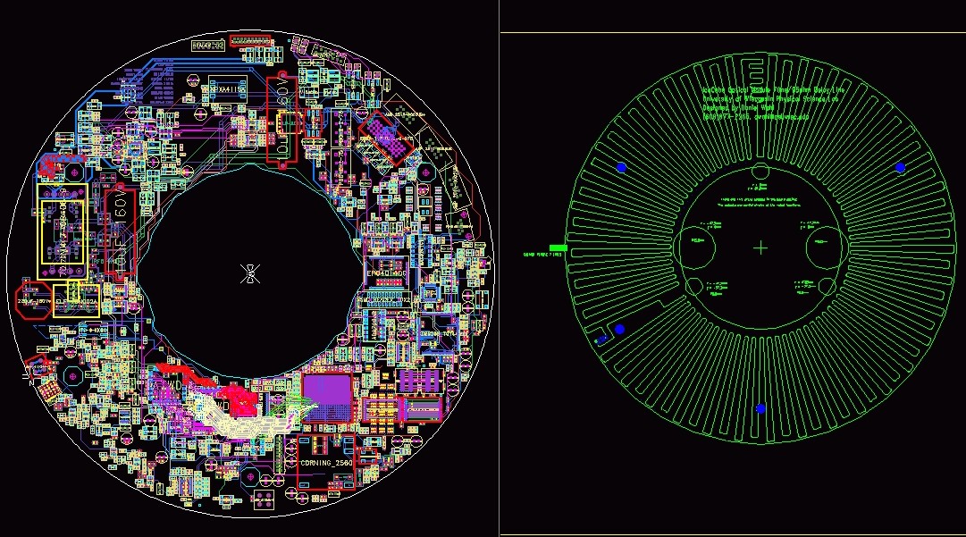
The locations of various cut-outs on both boards match up, so there
was no accidental flipping-over of one board with respect to the other.

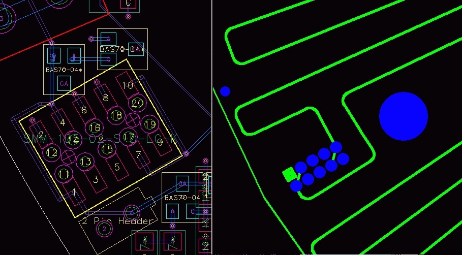
The signal pins on both the DOM MB and the Delay board match up.
JP5 on the DOM MB is confirmed by the layout tool to be on the back of
the board (Side 2)
(It was convenient to make the 10 pin connector a 20 pin connector
with overlapping pads to permit the pins of the header mounted on delay
card to be soldered to pins 11 to 20.)
Pin 1, the square pin, on the delay board suggests that the pin assignment for the connector is swapped side-to-side compared with a standard ribbon cable header, for instance.
The numbering doesn't count nearly as much as making sure the signal pins on one connector mate with the signal pins on the other connector.