Flasher Input Study
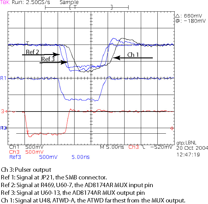
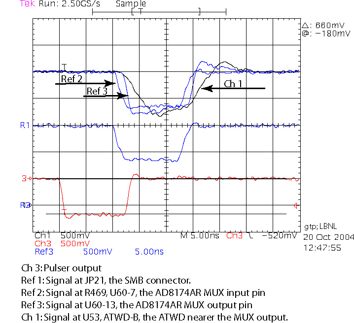
As can be seen from the images below, captured with a Tektronix TDS644,
and active, wide-band probes, the waveform at the input of the
multiplexer chip (Ref 2) is well behaved, compared to the signal
at the input connector. Likewise, the output pin of the mux's
internal amplifier waveform is a fairly faithful copy of the
input.. The degradation at the input pin of the ATWD (Ch1)
occurs as a result of the spread-out circuit traces on the board,
the fact that the output line is not resistively terminated, and from
the highly reactive input characteristics of the ATWDs.
(ATWD inputs appear at their input to be highly capacitive)
Furthermore, it was necessary to place a 25 ohm resistor between the
output pin of the Mux and the PCB traces in order to stabilize the
amplifier.


Mitigation proposal
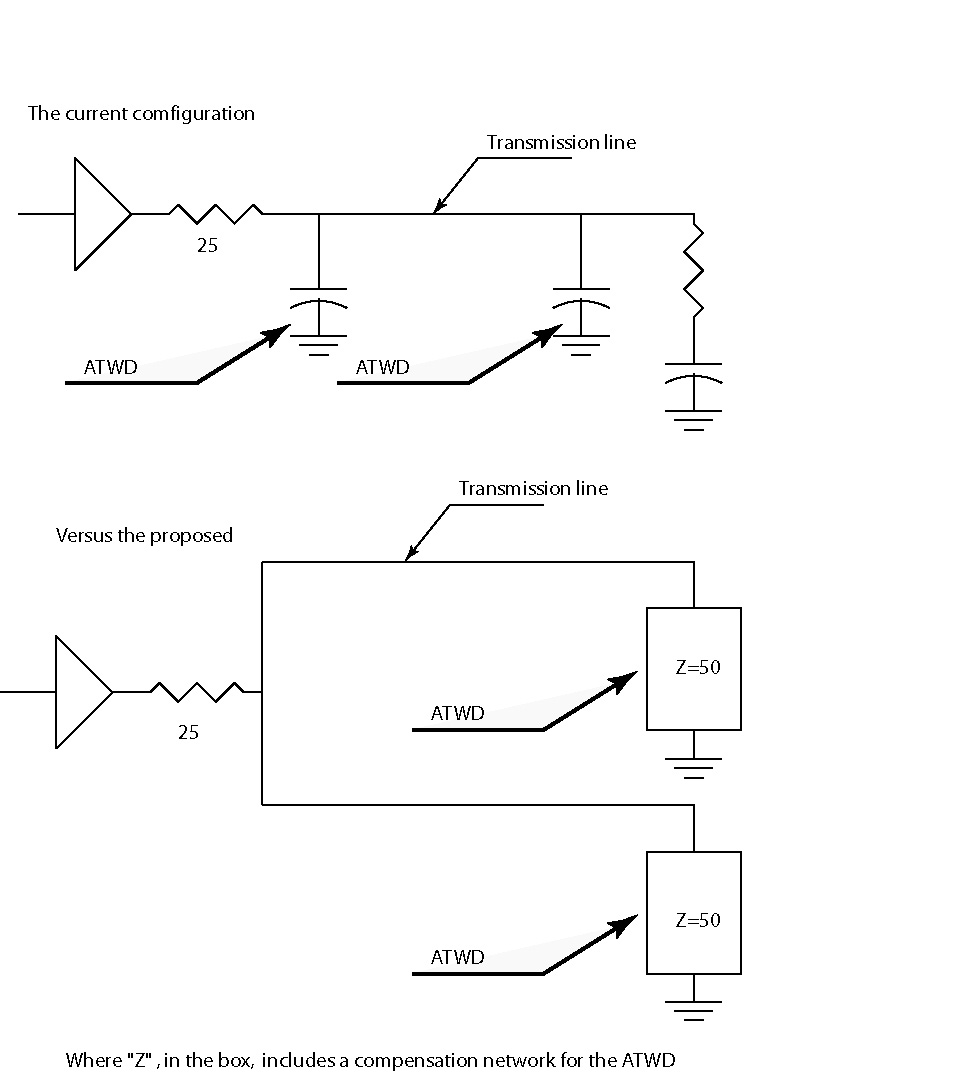
The waveform at the input of the ATWDs could be improved by providing a
pair of transmission lines, one to each ATWD, and by explicitly
compensating the reactive input of the ATWD pin, driven in parallel by
the MUX amplifier output.
The signal level at the ATWD input would be decreased by the voltage
division of the termination resistor and the back-termination
resistor. At low signal levels, the signal to (quantizaton)
noise ratio will decrease by a factor of 2.
Revisions included in DOM MB Rev 5.1 will not contain such enhancements.
If this deficiency is deemed to be serious enough to require
improvement, then they may be included in DOM MB Rev 6.0.
Before a termination can be proposed, it will be necessary to
characterize thedynamic (during acquisition) input impedance of
an individual ATWD input. This could be tricky, since the
acquisition takes about 1/2 microsecond.
for example:

10/22/04 G. Przybylski
