DOR Timing:

The GPS clock and DOR card as a System


For a collection of DOM Hubs to work together as a system which meets IceCube timing requirements, the DOR cards require a common 10 MHz clock signal, a 1 Hz (or 1 Pulse per Second) signal, and a time string signal from a GPS clock.  The firmware in the DOR card currently supports two GPS clock products: the True-Time model XL product line, and the Symmetricom model ET6000 product line.

Device topology in the FPGA of the DOR card imposes some timing limitations on the relative phase (skew) of the edges of the 1 Hz (1pps) signal with respect to the 10 MHz. Violation of the timing restrictions produces faulty FPGA behavior which propagates into the PCI device driver code in predictable and unpredictable ways.    Furthermore, the boundaries of the timing violation zones can vary somewhat from one firmware version to another because of changes in allocation and routing by the compiler of the resources inside the FPGA. 

Recommended Cabling between GPS Clock and DSB card

These recommendations should leave abundant safety factors relative phase of the 10 MHz and 1 Hz signal for any likely FPGA firmware version.  If a new firmware version suddenly produces unexpected behavior, then changing phase may be a useful diagnostic. 

When driving One to three DOMHubs from one ET6000 GPS clock, set as follows:
Observed timing, and recommended cabling for three DOMHubs highlighted in green
10 MHz GPS Output to lower LEMO connector on DSB
1Hz GPS Output to upper LEMO connector on DSB
Observed
1 Hz _↑‾  to 10 MHz _↑‾   timing (ns)
J5
J4
13.2
J5
J6
26.1 (recommended)
J5
J8
13.4
J7
J4
73.0 (recommended)
J7
J6
86.0
J7
J8
73.2
J9
J4
12.9
J9
J6
26.0
J9
J8
13.3 (recommended)

Kalle assures us that different sub-versions of DOR Rev 1 should impose roughly the same timing restrictions.

A short readgps test was conducted over the following timing ranges of   1 Hz ↑  to 10 MHz ↑ timing :

From
To
Behavior
67ns
95ns
Trouble free
8.0ns
31ns
Trouble free
3ns
4ns Violation for DOR Rev 0
5ns 8ns
Violation for DOR Rev 1

The timing regions which were found to be trouble free were checked with 1/2 ns granularity, for a duration of less than one minute. 
Regions with anomalous/faulty behavior were checked more extensively.
More extensive tests were taken with recommended configurations.  See the output page

South Pole Set-up Documentation

Documentation for 2005 (Temporary Counting House)

Background

GPS Clock Set-Up in the Bldg 50 Test Lab

A Symmetricom ET6000 provides the time signals for three DOM Hubs,  pirate-domhub, domhub1, and domhub-setup.  The timing signal distribution hardware most closely matches the configuration at the south pole, using splitters instead of individual cables from rear panel connectors on the GPS clock.
The Only domhub-setup has a full complement of DOR cards;  each hub has  at least one DOR card.

Measurements with a "typical configuration"

This configuration is one likely to be selected, by chance,  by a GPS clock user unfamiliar with the DOR timing limitations.
The test cables used to measure the skew of the DSB cards are all of equal length.
The scope trigger is the 1 Hz test point from one of the DSBs, and the remaining three scope inputs are the 10 MHz test test point from all three DSBs.

Clock skew:  CH1-to-CH2-to-CH3 skew in the 10 MHz signal < 350 ps total

The 1 Hz on J4 is supplied by MUX1 in the GPS clock
With 1pps from ET6000-J4, 10 MHz clock from J5,  1pps LH transition to 10 MHz LH transition  delay=12.8 ns
(square wave 10 MHz) (Mux2)
With 1pps from ET6000-J4, 10 MHz clock from J6,  1pps LH transition to 10 MHz LH transition delay=5.1 ns
(square wave 10 MHz) (Mux3)
With 1pps from ET6000-J4, 10 MHz clock from J7,  1pps LH transition to 10 MHz LH transition delay= 82.5 ns
(Sine wave 10 MHz)
With 1pps from ET6000-J4, 10 MHz clock from J8,  1pps LH transition to 10 MHz LH transition delay=12.45 ns
(square wave 10 MHz) (Mux2)

Affects of loading Changes

If one of the outputs from the fan-out is disconnected, the timing will change a little depending on whether the 10 MHz source is a sine wave or square wave.
i.e. removing one of the 10 MHz output cables from the splitter will cause a shift of 150ps if the 10 MHz is square wave,  but a whopping 1.33ns if the 10 MHz is a sine wave.

Affects of 1 Hz signal to clock signal skew on Serial String processing in DOR

  (The skew of the 1Hz test point and 1Hz test point in the DOR FPGA, with respect to the 10 MHz clock, have not been measured)
Experiments done with pirate-domhub, which is a DOR Rev1 (no suffix), card0, running pci-7, FW=101i,

When 10 MHz clock rises 7.98ns after Hz, as measured at the rear panel of the DSB, the clock decoding is OK.
When 10 MHz clock rises 7.76ns after Hz, as measured at the rear panel of the DSB, the clock decoding is faulty occasionally
When 10 MHz clock rises 7.54ns after Hz, as measured at the rear panel of the DSB, the clock decoding is faulty most of the time
When 10 MHz clock rises 5.46ns after Hz, as measured at the rear panel of the DSB, the clock decoding is faulty occasionally
When 10 MHz clock rises 5.24ns after Hz, as measured at the rear panel of the DSB, the clock decoding is gets occasional extra zero bytes, but on 20M-1, 20M+1 pairs.b

Experiments done with pirate-domhub, which is a DOR Rev0, card5, running pci-0, FW=010w

When 10 MHz clock rises  4.1ns after Hz, as measured at the rear panel of the DSB, the clock decoding is OK.
When 10 MHz clock rises  4.0ns after Hz, as measured at the rear panel of the DSB, the clock decoding is occasionally faulty
When 10 MHz clock rises  3.16ns after Hz, as measured at the rear panel of the DSB, the clock decoding is still occasionally faulty.
When 10 MHz clock rises  3.0ns after Hz, as measured at the rear panel of the DSB, the clock decoding is OK.

This identifies the forbidden timing regions.

Test configuration:


10 MHz source
1Hz source
1 Hz _↑‾  to 10 MHz _↑‾   timing (ns)
J5
J4
13.1
J5
J9 13.3
J6
J4
5.4 (Forbidden)
J6
J9
5.8 (Forbidden)
J7
J4
72.9
J7
J9
73.2
J8
J4
13.0
J8
J9
13.2
The two cells highlighted in read indicate that a FPGA timing violation condition exists for the Rev 1 DOR card and current firmware.

Skew in Distribution

Inside the DOM Hub

For this test, the cable lengths were tuned to produce a reference skew between 1 Hz and 10 MHz LH transitions, as observed at the DSB.
These measurements were  made in  the Building 50 Test Lab.
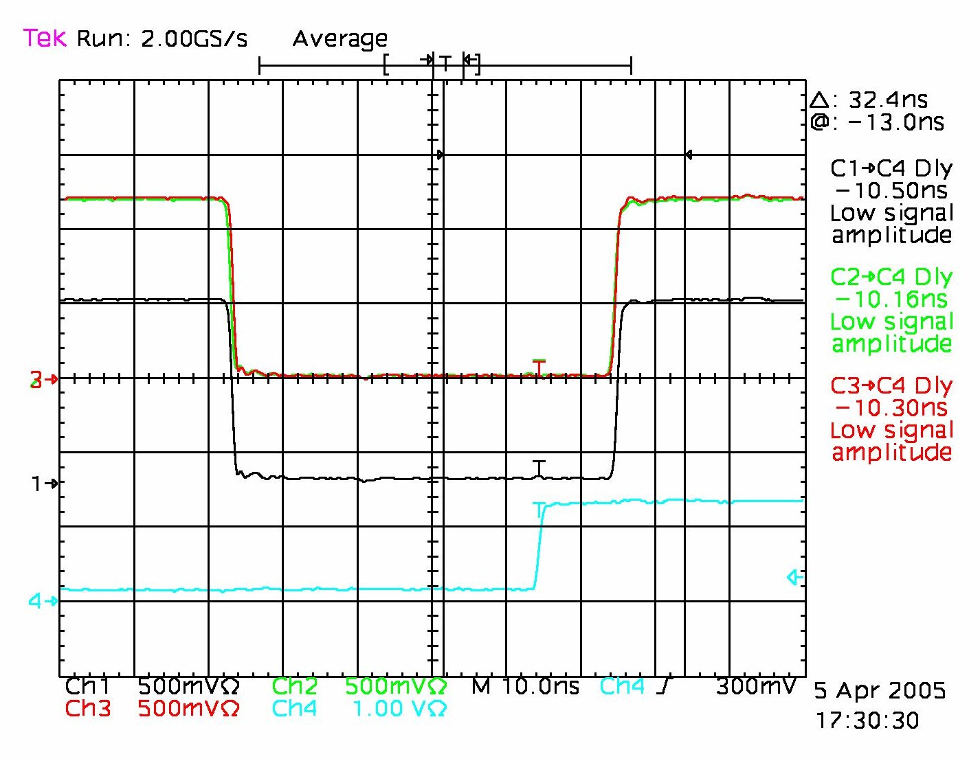
1Hz to 10 MHz Clock Skew at DSB JP4
1Hz, 10 MHz, and 20MHz clock skew in DOR
DSB_1Hz-to-10MHz_skew
DOR_1Hz-to-10MHz-to-20MHz_Skew

G. Przybylski mailto
Lawrence Berkeley National Lab
Comments? Trouble reports?