DOM Testing Visuals... Apologies for the poor quality of some of the photographs.

Master Clock Simulator

Master Clock Simulation Breadboard


Schematic for MCU input simulator 
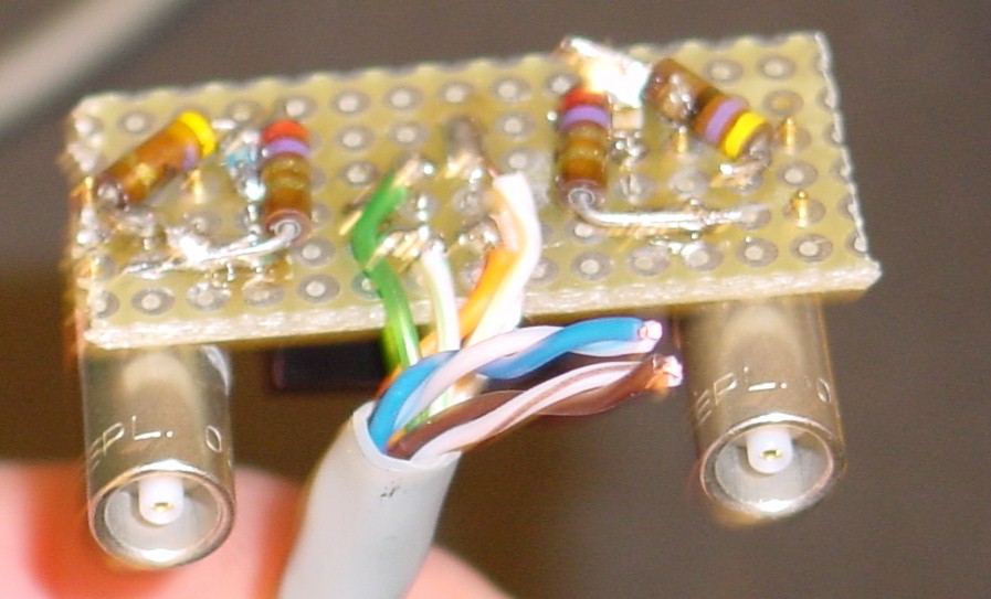
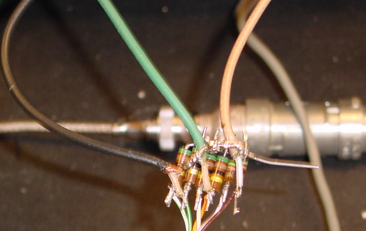
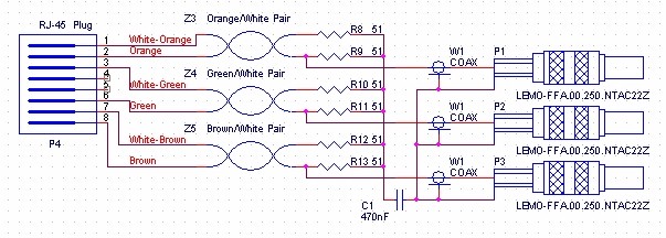
The breadboard circuit matches to a 50 ohm 3V source (a typical GPS clock BNC output characteristic),  to a 100 ohm  low level load.  The voltage division of the resistor network on the left yields approximately 0.16V at the input to the transformer.  The transformer ratio turns that input voltage into approximately 90mV at the twisted pair.  The signal from this breadboard is coupled into comparators in the DSB that drive the fan-out.  The low input level  delivered by this matching unit is a relatively good sensitivity test of the DSB comparator inputs.

The equations (for Maple) are:
solve({300=R2+(((R1+50)*R3)/(R1+R3+50)),50=R1+(((R2+300)*R3)/(R2+R3+300)),0.1615=3*(((R2+300)*R3)/(R2+R3+300))/(R1+(((R2+300)*R3)/(R2+R3+300)))},{R1,R2,R3});
which yielded values of  R1 = 47, R2 = 297, R3 = 2.7 for the matching circuit.  47ohms, and 2.7 ohms were readily available, however, 294 ohms was the nearest to 297 ohms.  Transformers on the bottom of the breadboard match 300 ohms(@0.16V) on the input side to 100 ohms (@90mV) on the twisted pair side.

DOR Simulator:  Matching LVDS outputs of the DSB card to Oscilloscope inputs

DOR card like LVDS Termination

Well... 'DOR simulator' is a bit of a stretch... It's really only a haywired-in-the-air termination for three LVDS pairs, combined with short cables that can be plugged into an oscilloscope


LVDS Terminations
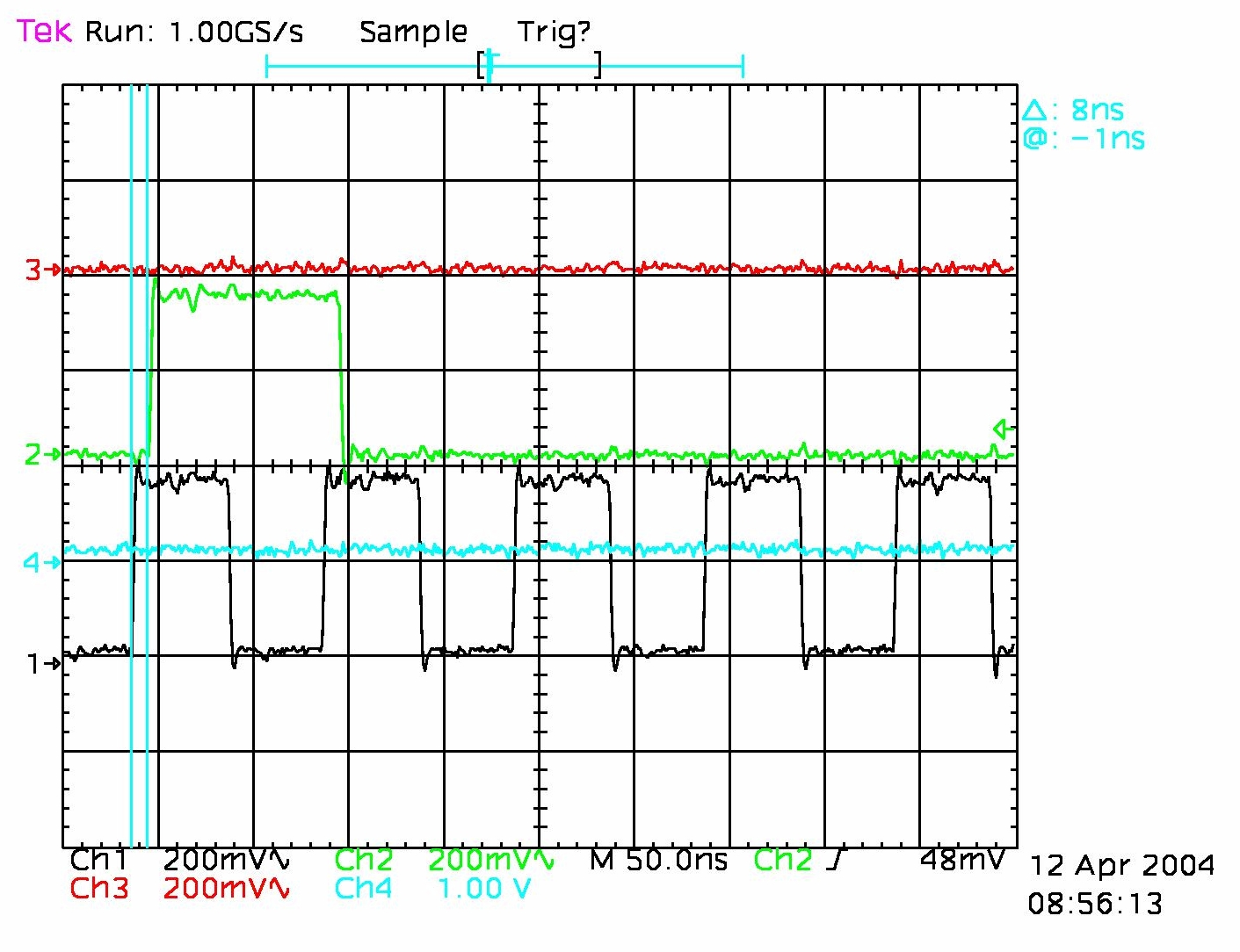
The LVDS signals are differential, so the breadboard circuit is designed terminate the 100 ohm characteristic impedance of the Cat-5 cable with resistors to a common point, which floats up to the mid point of the differential voltage.  To monitor the outputs, plug into a scope with the inputs set to 1M termination impedance, 100mV/div,  and AC coupling.

CPU board Power

DSB Testing Power Supply

3.3V on Orange, Ground on Black, and 5V on Red.  No other voltages are needed by the CPU board for this test..

Modified CPU board

3.3V connectins on back of CPU MB

PCI connections to 3.3V

Set Up

Test Setup

The 'customized power cable' provides power from the power supply on the left to the ATX power socket on the mother board.  The marked PCI socket is wired with 3.3V power from the ATX connector.  The DSB card under test is inserted into the marked socket.  The connections shown on the lower edge of the picture are to the GPS clock inputs, and the MCU input (the RJ-45 connector).   The null modem cable from the GPS clock, or a computer plugs into the black Dsub-9 at the top of the PCI panel.   The performanceb can be monitored by probing the board with an oscilloscope, or by observing the outputs of at the end of the cable plugged into the black multi-output ports at the top of the card.

Cut Trace

Where to cut the PCB trace

Pulse in response to push button, or closure across header pins

10 MHz and 1pps timing

The trace on channel 2 is the 1pps output at the LVDS terminator.
Trace 1 is the 10 MHz output at the LVDS terminator.
The pulse is induced either by depressing and releasing the rear panel switch, or by placing a momentary short across the top two contacts of the rear panel header.