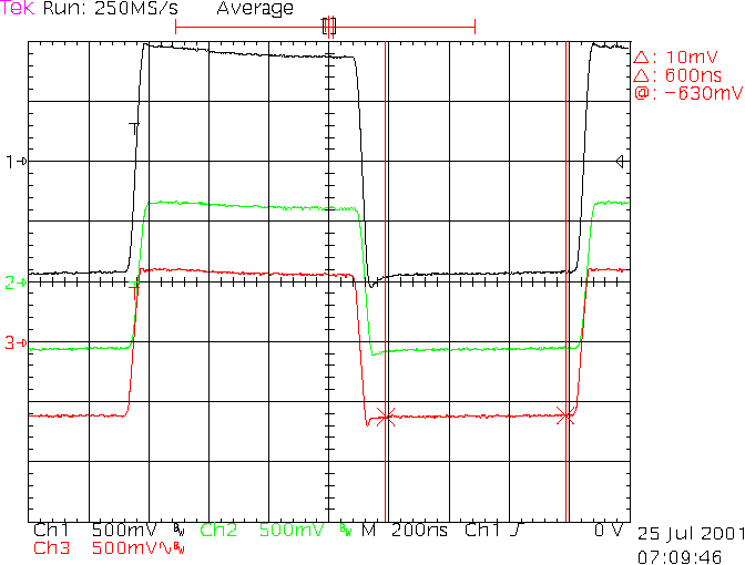
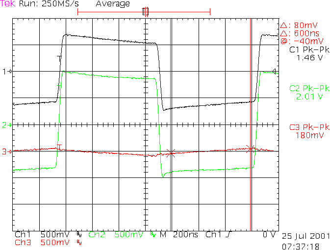
In the screen snap below, the current of 50 mA injected into the
common port of the splitter
divides evenly to each side port. The bias current has some affect
on the inductors in the
splitter, causing the signal to sag an additional 2%
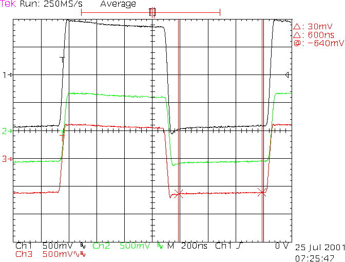
Distributing 100 mA (50 mA per side port) results in an additional
4 % sag as seen below.
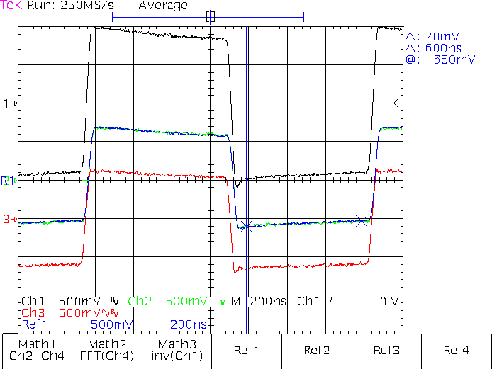
If the DC path to one side port is interrupted, the impact on the waveform
is negligible, as can be seen
by the superimposed traces Ref-1 and Channel 2.
When current is applied to the common port, and a simulated communications
signal drives one
of the side ports, a low amplitude triangle pulse appears at the other
side port. The origin
of the triangle waveform is not yet completely understood.
No show stoppers so far.