The HomePage for DOM Service Board (DSB) Testing
Follow the links. They are full of good stuff
History
The interested parties, at a relatively high level, at LBL and
UW, arranged for Gerald Przybylski to create schematics, and
specify components for the DSB. The schematic was entered
into OrCAC Capture.
The (revised) schematics were
handed over to Dan Wahl, and Howard Mattison, at UW to create a layout
using the net list created by OrCAD for the PADs layout tools
used
by Wisconsin.
Upon completion of the layout, the Gerber files were handed over to an
EMS vendor for PCB manufacture, and component
loading.
Preliminary check-out was done by Harold Mattison, in Wisconsin, (where
two boards were retained) before the remainder were sent to Berkeley
for integration into the next batch of DOM Hubs.
The original OrCAD schematics have
been revised to match the "As Built" DSB cards.
Component Changes
Z1 through Z4, Ferrite Chip beads in an 1812 package should be replaced
either with Delevan EMI-1812-125,
or Steward MI1812K121R-00 of the style in Figure 2. These
have lower DC resistance than the ones provided by the EMS house.
Delevan is on the QML, and Steward is not.
Lift pin U2-1, or remove U2 if the CPU board will supply 3.3V to pins
on the PCI connector. If 5V only is available, I am
skeptical that U2 can source enough current without overheating (it's
only an 8 pin SOIC chip).
Cut circuit trace at the location depicted in this image.
Installation Requirements
- PCI mother board and power supply, or passive backplane and power
supply, with 3.3V connected to PCI connector socket pins 25, 31, 36,
41, 43, 54. (Brad... please check on this) (See Modified CPU board)
- For checking the GPS clock inputs, a GPS clock with 10 MHz (or RF
generator or synthesizer), 1 pulse per second (or pulse generator), and
RS-232 output (or a computer serial port, and terminal emulator
program) and null-modem cable.
- For checking the Master Clock input, a Master Clock, or a Master Clock Input simulator, and
either a GPS, or RF generator and pulser, as above.
- To observe the outputs, either a scope probe, and schematic, or a DSB termination simulator.
- Power for the CPU board. (see test
config)
Check-Out at LBNL
The test set up, next to the
oscilloscope, allows powering, applying stimulus, and observing outputs
from a DSB under test.
If a DSB does not have either a Toyocom, or Corning oscillator,
and the card will be used in a stand-alone configuration (without an
MCU or GPS input) then one must be installed before proceeding.
Results
- 100 % of the DSB units behaved as expected, delivering clock
output from the internal oscillator, and auto-switching when an
external GPS clock output was plugged into the 10 MHz input.
- The 1 pulse per second signal applied to the GPS or MCU input was
delivered to the fan-out as expected. (See quirk below)
- A single pulse is induced by either depressing the on-board
switch, or jumpering the top two pins of the rear panel header.
Timing is 8ns. See single
pulse waveform.
- The serial fan-out from the RJ-45 has been shown to work,
however, a test with the MCU input has not yet been conducted, since
and RS-485 source was not be readily available (but RS-232 should also
work).
Features/Documented 'Bugs"
The testing set-up for monitoring the LVDS outputs should have
individual bypass capacitors, since all outputs are not 50% duty cycle.
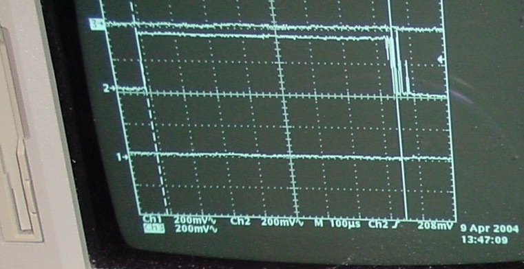
The leading edge of the waveform (at dotted cursor mark) is well
behaved, however, for input pulses longer than about 700 us,
the.trailing edge will misbehave (metastability) (see image
above)
as the comparator threshold drifts toward the input voltage, and the
comparator input sags.... This feature imposes a
requirement on DOR firmware that, re triggering must be inhibited
beyond the period when metastable operation can occur.
Pulses as short as one or a few clock cycles behave well.
The standard 1pps clock output of a GPS clock (approximately 20us) will
behave well. A 50% duty cycle clock will misbehave. A
future DSB, with an embedded logic device, will exercise better control
on the output pulses.
No other problems are known at this time.
April 9, 2004 gtp