
This page might be clarified by examination of the DOM MB block diagram.
The DOM Main board utilizes a synchronous triggering scheme. Incoming pulses from the photomultiplier tube are detected by a comparator (U54 or U58). The output from the comparator initiates a state machine in the FPGA which, on the next reference edge of the 40 MHz internal clock time-base, causes the clock counter value (=time-stamp for the hit) to be captured, as well as sending the a trigger (launch) signal to be ATWD.
Trigger signals to the ATWD have an absolutely fixed relationship with the time-stamps of hits from the PMT. However, the ATWD sample number of the pulse rising edge in the ATWD record is not fixed. It varies over a range of 25ns, with some noise allowance on both edges.
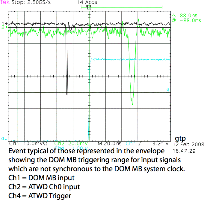
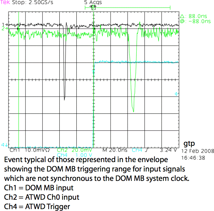
This sampling of two individual events show the fixed time relationship of DOM MB input to ATWD signal due to the delay line, propagation through amplifiers, and pc-board traces (obviously), compared to the uncorrelated relationship of the ATWD trigger signal to the DOM input:
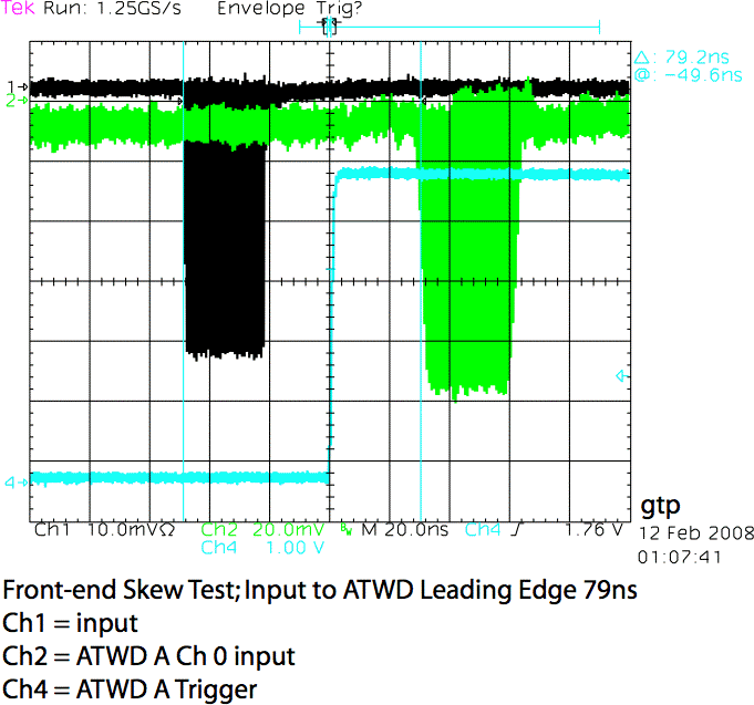
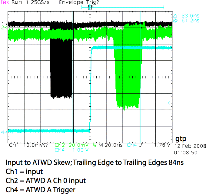
Except for the calibration screen snapshots, the timing profiles below are built up of overlays of many, many events like the two shown above. The oscilloscope triggers from the ATWD Capture signal, Ch4. The Ch1 and Ch2 traces are built up from an overlay of many events (the "Envelope" display mode for the oscilloscope).

Since the oscilloscope is in Envelope capture mode, the black splotch at the left is comprised of an overlay of many inputs, each with random time relationship to the DOM MB clock. The green spltch is slightly broader because of degradation of the signal passing through the delay line and amplifiers on the way to the ATWD.
The leading edge delay from the black to the green splotch arises from the propagation through the delay line and amplifiers to the ATWD input. On-board delays are small compared to the delay line.

The cursors are set to the trailing edge of the input and ATWD signal profiles.
The cursor shows the time relationship of the input with respect to the trigger plus 1 whole clock cycle plus the width of an input pulse plus the minimum delay from trigger to ATWD capture.
49.6 - 25.00 - 2 = 22.6ns = minimum input to trigger set-up time
Direct measurement of the minimum propagation delay from the main board input into the trigger comparator into the FPGA to the ATWD trigger input. [The edge of the black blotch of Ch1 input signals to the cyan Ch4 ATWD trigger signal.]
Probe calibration:
The DOM MB trigger comparator trips when the signal is only a few mV above baseline. Therefore, it is probably better to match leading edges rather than the peaks of these waveforms. A 0.5ns to 1ns correction may be called for.
February 12, 2008 gtp lbnl