AMANDA String 18 Information
This page contains some of the documentation for the Digitial Optical Module string, AMANDA string 18. String 18 consists of 42 optical modules. The bottom 40 are digital, with integrated fiberoptic drivers that feed into the AMANDA fiber receiver cards. The remaining two optical modules are typical AMANDA fiber modules (or might be DaOM).Schematics:
The string 18 DOM Flasher Card
The string 18 DOM schematics from LBNL, DAQTestBoard schematics from LBNL, and DOMCOM schematic from Karl Heinz Sulanke, DESY Zeuthen, based on the DAQTB
The AMANDA string 18 readout upgrade project.
As of May, 2001, the plan is to build on the experience of the four
test board system installed at the south pole in January 2001 by Azriel
Goldschmidt, Jodi Lamoureux, Chuck McParland and Gerald
Przybylski. The test board, however, requires some redesign, as
described in the test board
redesign plan.
The redesigned board will then have to be fabricated, tested, packaged, and tested again by a team of collaborating institutions which, as of May 16, had not yet committed to the components of the project. The straw man project breakdown proposed here is a starting point for dividing up the project into chunks which fit with the capabilities and goals of the various collaborators.
The May meeting reached consensus on going forward with the project as an AMANDA initiative with various responsibilities spoken for based on interest and resources available.
As promised the slightly modified test board schematics are provided, June 11, along with a preliminary layout, another binary, to Karl-Heinz Sulanke, DESY Zeuthen, for layout and fabrication (see also the note). Shortly thereafter, a revised schematic and layout were completed. Karl-Heinz indicated that he took the schematics in hand, and modified them to place two channels on one card, and changed the computer bus connector from PC-104 SBC style to a standard ISA card edge connector. In the mean time, Jean Paul DeWulf requested the a layout, and schematics, and Gerber files (PCB fabrication files) which use the existing PC-104 style connector (available June 28).
Of course, the other half of the project is a set of firmware design files, and an applications programmer interface document. The first describes the logic configuration inside a field programmable gate array (FPGA). The second describes how a programmer controls the functionality of the 'firmware'. The API document and the related firmware are likely to continue evolving as collaborators progress down a list of new features. Every effort will be made to keep the firmware and software running at the various collaborating institutions compatible with cross fertilization among the groups.
Short comment on Hardware
Both the DOMCOM Test Board and the DOM use the same clock frequency for timing and to clock synchronous logic. The DOM oscillator is not, however, phase locked to the frequency of the surface electronics. The communications grade temperature compensated crystal oscillators in the DOM exhibit remarkably small Allen Variance (about 6E-11), and low drift in the virtual 'oven' that is the sphere thousands of feet deep in the antarctic ice.The time synchronization of events or hits collected by different DOMs depends upon tracking the oscillators in the DOMs with respect to a common reference. Each DOM clock frequency, drift, and phase is tracked by surface data acquisition electronics and programs through the exchange of timing events over the twisted pair cable. Absolute times and clock drift data are merged into the event data stream for off-line analysis. For string 18, the synchronization of all incoming events depends upon all DOMCOM boards clocking in lock step. That requires a common reference clock.
The String 18 Reference Oscillator Subsystem (referred to as clock unit subsequently in this document), contains a Rubidium oscillator coerced by a one pulse per seconds signal from a GPS receiver to track the oscillator at the Naval Observatory, the reference clock for GPS. The stability of the rubidium oscillator exceeds that of GPS by three orders of magnitude in the one to ten second time window so crucial to the tracking of DOM stability. In the clock unit, the rubidium oscillator drives a phase locked loop IC, which produces the appropriate clock frequency for the DOMCOM Test Boards. The PLL output drives a tree of "zero delay buffer" ICs which fan the signal out to a separate port (individual driver IC) for each DOMCOM Test Board through equal length twisted pair cables..
The one pulse per second output from the Rubidium oscillator fans out to each of the DOMCOM Test Boards through an FPGA. The FPGA loads from configuration memory on power-up. Fanning out the one PPS signal through the FPGA allows great flexibility, including the tuning of time delay to each output, and the 'slipping' of the one PPS pulse to a different clock cycle, for instance. Reconfiguration after boot may be done from a computer over a parallel port cable, allowing for replacement of the default configuration with one motivated by further software or firmware development.
Different pairs of the four pair Category 5 cable carry the 16.8 MHz signal and the one pulse per second signals from the clock unit to the DOMCOM Test Board. The twisted pairs cable has low susceptibility to noise and EMI pick-up. DOMCOM Test-Boards occupy slots in the Wisconsin industrial PCs.
Each DOMCOM Test Boards contains a PLL IC which delivers 16.8 MHz and 33.6 MHz matched in phase to the 16.8 MHz reference. Synchronous logic in the FPGAs clock with these clocks, as does the communications ADC and DAC. Timing tick waveforms captured with the communications ADC, or generated with the communications DAC are 'time stamped' by latching the internal 33.6 MHz clock counter for subsequent read-out. When the FPGA is placed in the proper state, the one pulse per second signal triggers resynchronize the system by forcing the clock counter to zero counts. Otherwise, each one PPS tick causes a register to latch clock bits. These periodic clock samples, when compared across all test-boards, allow the detection of time synchronization faults.
The Reference Oscillator Subsystem
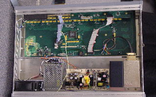
was completed in Berkeley, tested briefly, and flown to the south pole station, where it is installed (see also installation details) in the counting house.