Common Clock Tests
Background
The measurement of the propagation time from DOR to DOM, and back, utilizes time measurement and transfer hardware, firmware and software, built into the DOM, and DOR cards. Pulses sent by the DOR card are digitized by the DOM, and vice-versa. The firmware on both ends time-stamp the transmission, and reception of pulses. The data are analyzed in the string processor to extract the round-trip time through the wire pair, the clock counter offsets between the DOM and DOR, and the relative frequency differences between the DOR and DOM counters.
The clock correction for the DOM is half the round-trip time from DOR to DOM and back.
In order to explore systematics, like asymmetry in the round-trip measurements, and time off-sets in hardware and firmware, it is useful to clock both the DOR and DOM main board from the same clock source, namely, a particular DOR card... with the clock on both boards in phase, or, at least, with fixed, constant phase between them.
Normally, the DOM MB utilizes a crystal oscillator as its local frequency reference source. The common clock tests require the replacement of the oscillator module with a module that processes clock fan-out signals from the DSB card as replacement for the oscillator. A further enhancement to this substitution is the distribution of the 1 Hz time reference signal to the DOM MB, since it is present on the cable from the DSB card.
The clock pick-up card
The clock pick-up card consists of LVDS line receivers on the 1-2, 3-6, and 7-8 pairs of the RJ-45 cable, delivering 10 MHz, 1Hz, and serial signals to pins on a card with the same footprint as the Y1 oscillator module. (The serial time-string signal is not necessary for the tests, so those components are not loaded)
The 1 Hz receiver on the pick-up card delivers its output to a test pin which is connected to a spare pin of the DOM FPGA. Customized firmware captures the internal clock counter value after every positive going transition of the 1Hz clock signal. The firmware makes the value available to the software API, where it can be read, and transferred to logging software.
The 10 Hz receiver drives the input of a Phase-Lock Loop chip (PLL), which doubles the frequency to 20 MHz, as required by the PLLs and other electronics on the DOM MB. In order to assure that the
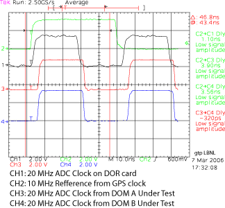
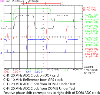
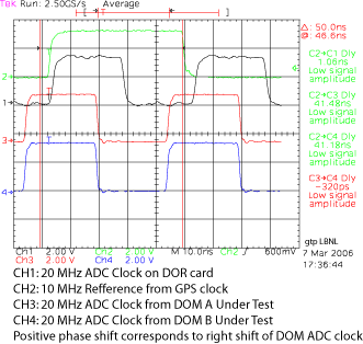
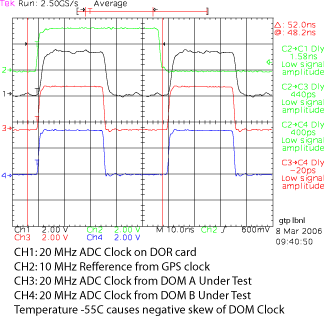
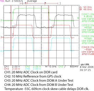
20 MHz duty cycle is 50%, the resources in the PLL chip are configured to operate the internal voltage controlled oscillator (VCO) at a multiple of 20 MHz, then divide the signal down to 20 MHz. The device happens to implement a multiply by 8, divide by 4 scheme, which has the side-effect of locking in one of four possible phase relationships with respect to the reference signal imported from the DSB card.
| in-phase |
+90 degrees |
+180 degrees |
+270 degrees |
 |
 |
 |
 |
down - up = 36.74 (36.96) ns
average = 1055.20 (962.55) ns |
down - up = 10.08 (10.25) ns
average =1053.50 (961.50) ns |
down - up = 87.32 (87.44) ns
average = 1053.52 (961.50) ns |
down - up = 62.52 (60.91) ns
average = 1054.25 (961.66) ns |
|
|
|
|
in-phase at -55C
DOM phase shifted left due to temperature |
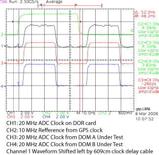
in-phase at -55C with 609mm skew cable |
in phase
DOR phase shifted right due to 609mm skew cable |
|
 |
 |
 |
|
down - up = -5.14 (-5.70) ns
average = 1026.55 (935.26) ns |
down - up = 2.42 (0.22) ns
average = 1025.90 (935.12) ns |
down - up = 6.80 (7.20) ns
average = 1030.11 (937.49) ns |
|
Values in parenthases are for "B" DOMs, which are located 17 meters from the end of the cable.
Objectives:
Measure RMS uncorrupted by relative clock drifts
Measure one-way time down
Measure one-way time up
Measure dependance of round-trip time and RMS on temperature under controlled conditions
Measure the effect of 17 meter break-out cable.
Measure the effect on asymmetry of having DOM B present or absent during measurement.
Measure the dependance of round-trip time and RMS on absolute cable length
Data Files
Results spreadsheet
The data files are compressed into a tar archive available here.
The file name-to-conditions mapping is available here (soon).
Goals:
Quantify phase delay between GPS clock, and DOR card 1pps time-tick time-stamp arising from process hidden in electronics and firmware
Quantify and/or Calibrate the time synchronization process between DOR and DOM under controlled conditions.
Identify any anomalies in the IceCube process of time-transfer to the DOM time-frame.
