The Rev 5.1 Production Page, 2005
Running Totals for Delivered boards:bv
For delivery totals, Ask Azriel, or Bill Edwards (totals to Wisconsin, Zeuthen and Sweden)
For assembly house delivery totals, ask Azriel, or Jimmie
For testing rejects, ask Azriel, or Billie, or George to get the numbers out of the database...
| Analysis Pending |
Repaired
Pending
|
Repaired
Shipped
|
Software Test
Only
|
Unrecoverable
|
250
|
|
?
|
2
|
?
|
Updated 6/3/05
Actions Taken
Repeat problems, and production issues have prompted certain actions. Description: Here
As noted in the description of repeated problems, several could be solved by changes to software, or changes to firmware. No rework was required on these boards. Boards recovered by software and firmware fixes make up a substantial fraction of board problems.28
Rev 5.1 DOM Main Board Repair History
The boards entered in this list failed either an inspection, or a performance test.
* This list isn't comprehensive; it does not include boards diagnosed in the test lab, and routed for replacement of ATWDs, and serial ADCs, or that were recovered by software or firmware enhancement.
The analysis and repair work on Non-Conforming is summerized below.
The details links are based on the Template Repair Record form; Report forms are here.
Repair records for DOM MBs debugged in the Second year
- #1148 March 24, 2005 -- Fails Tests at -50°C
- Details
- #1010 March 10, 2005 -- Fails disc scan and fADC baseline test at -50°C
- Details
- #1016 March 10, 2005 -- Low current when first powered up
- Details
- #1018 March 10, 2005 -- Cannot load flash image
- Details
- #1134 March 18, 2005 -- Cannot load flash image
- Details
- #1256 March 31, 2005 -- Cannot run STF
- Details
- #1258 March 31, 2005 -- Cannot load flash image
- Details
- #1314 April 6, 2005 -- Low voltage; high current
- Details
- #1335 April 8, 2005 -- Cannot communicate
- Details
- #1347 April 19, 2005 -- Low Power Supply Current
- Details
- #1411 April 8, 2005 -- Cannot access EPXA4 JTAG chain
- Details
- #1425 April 19, 2005 -- Cannot communicate
- Details
- #1448 April 19, 2005 -- Low Power Supply Current
- Details
- #1477 April 19, 2005 -- Cannot load flash image
- Details
- #1028 April 19, 2005 -- Local Coincidence Loopback Test Failure
- Details
- #1033 April 19, 2005 -- Local Coincidence Loopback Test Failure
- Details
- #1145 April 19, 2005 -- Pressure reading incorrect
- Details
- #1245 April 19, 2005 -- Local Coincidence Loopback Test Failure
- Details
- #1248 April 19, 2005 -- Pressure reading incorrect
- Details
- #1302 April 19, 2005 -- Local Coincidence Loopback Test Failure
- Details
- #1311 April 19, 2005 -- Local Coincidence Loopback Test Failure
- Details
- #1344 April 19, 2005 -- Pressure reading incorrect
- Details
- #1361 April 19, 2005 -- Pressure reading incorrect
- Details
- #1086 March 16, 2005 -- Pressure reading incorrect
- Details
- #1382 April 19, 2005 -- Pressure reading incorrect
- Details
- #1074 April 19, 2005 -- Pressure reading incorrect
- Details
- #1388 April 19, 2005 -- Local Coincidence Loopback Test Failure
- Details
- #1400 April 19, 2005 -- Pressure reading incorrect
- Details
- #1451 April 19, 2005 -- Pressure reading incorrect
- Details
- #1465 April 19, 2005 -- Pressure reading incorrect
- Details
- #1142 April 19, 2005 -- Long Memory1 Test Failure
- Details
- #1173 April 19, 2005 -- STF Hang during Temperature Test
- Details
- #1294 April 19, 2005 -- ATWD Pedestal failures
- Details
- #1307 April 19, 2005 -- STF Hang during Temperature test
- Details
- #1339 April 19, 2005 -- ATWD Chip B Pedestal test failures
- Details
- #1463 April 19, 2005 -- ATWD A Pedestal test failures
- Details
- #1497 April 19, 2005 -- ATWD A Pedestal and Pulser test Failures
- Details
- #1090 March 15, 2005 -- ATWD and fADC Pulser Test Failures
- Details
- #1310 April 19, 2005 -- ATWD Pulser Test Failures
- Details
- #1446 April 19, 2005 -- ATWD and fADC Pulse failures for all tests
- Details
- #1492 April 19, 2005 -- ATWD sweep and pulse failure
- Details
- #1285 April 19, 2005 -- ATWD Pulser Test Failures
- Details
- #1472 April 19, 2005 -- ATWD and fADC Pulser Test Failures
- Details
- #1442 April 4, 2005 -- ATWD and fADC Pulser Test Failures
- Details
- #1105 March 18, 2005 -- ATWD and fADC Pulser Test Failures
- Details
- #1197 March 23, 2005 -- ATWD and fADC Pulser Test Failures
- Details
- #1312 April 4, 2005 -- ATWD and fADC Pulser Test Failures
- Details
- #1476 April 21, 2005 -- ATWD and fADC Pulser Test Failures
- Details
- #1749 April 19, 2005 -- ATWD pulser, disc_scan, fADC baseline failures at -50°C
- Details
- #1758 April 19, 2005 -- ADC and pressure test failure cold
- Details
- #2241 April 19, 2005 -- Local Coincidence Loopback Failure
- Details
- #2285 April 19, 2005 -- Local Coincidence Loopback Failure
- Details
- #1073 March 3, 2005 -- Local Coincidence Loopback Failure
- #1073 May 20, 2005 -- ADC reading failre. U8
- Details
- #1357 April 6, 2005 -- Pedestal Noise Chip B Ch 0,1,2
- Details
- #1912 April 19, 2005 -- Missing B/I Test Printout
- Details
- #2292 May 23, 2005 -- Dropped from 4 feet
- Details
- #1002 March 10, 2005 -- Pressure reading too low
- Details
- #1045 March 10, 2005 -- Clk 1x failure on both ATWDs
- Details
- #1092 March 3, 2005 -- Download failure. Low current
- Details
- #1433 March 10, 2005 -- Clk 1x failure on both ATWDs
- Details
- #1115 May 23, 2005 -- Non Conforming. Lifted Pad
- Details
- #1170 March 22, 2005 -- fADC Baseline symptom
- Details
- #1371 March 22, 2005 -- Cannot read ID. Input current wrong.
- Details
- #1025 March 14, 2005 -- Excessive power consumption; Dead
- Details
- #1015 March 25, 2005 -- SDRAM Memory Failure Cold
- Details
- #1043 March 25, 2005 -- Failure to communicate at all temperatues
- Details
- #1057 March 25, 2005 -- SDRAM Memory Failure Cold
- Details
- #1071 March 24, 2005 -- Discriminator Scan Failures Cold
- Details
- #1105 March 18, 2005 -- Many fADC and ATWD STF failures
- Details
-
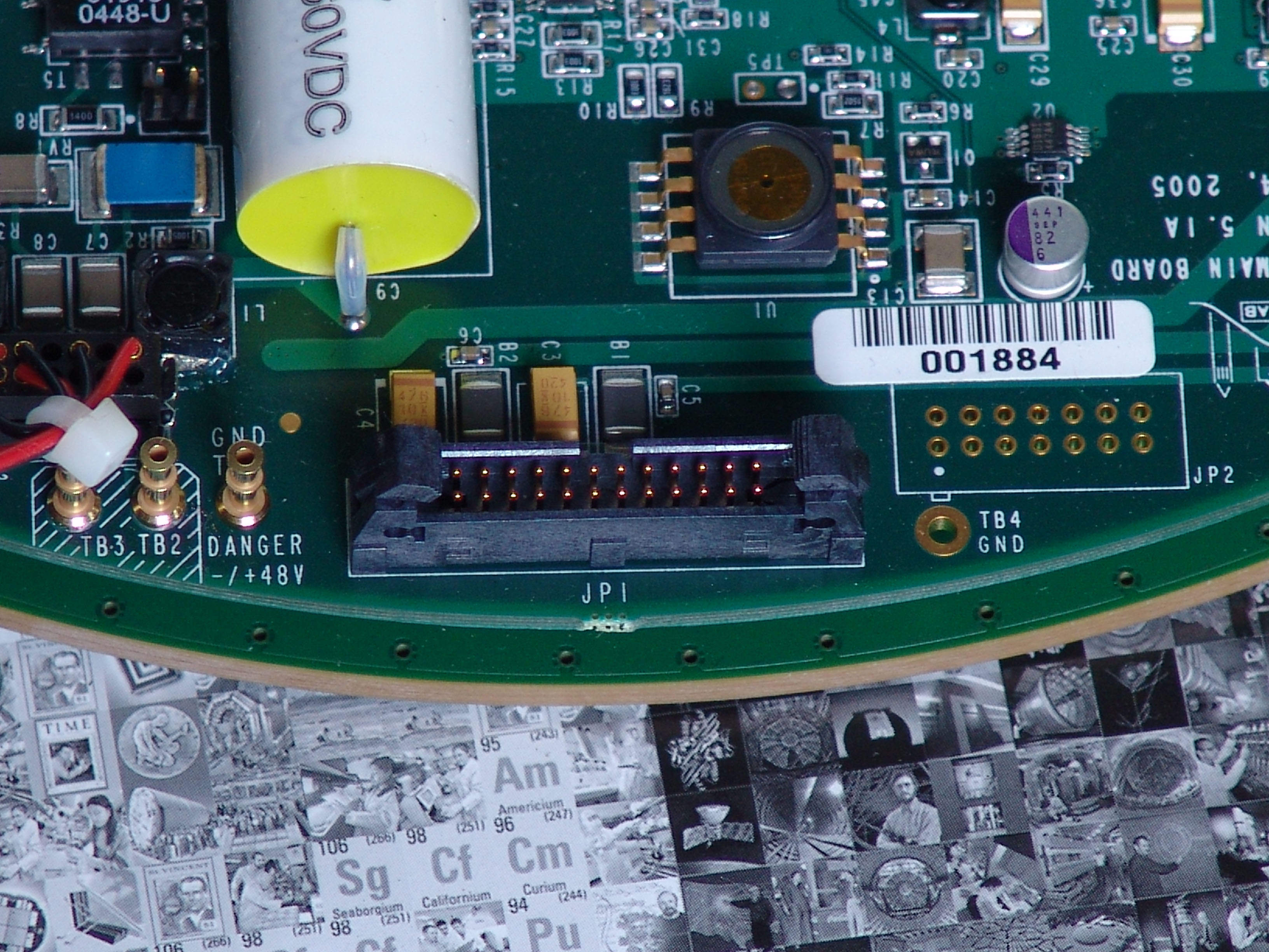
JP1 Rework, December 2006
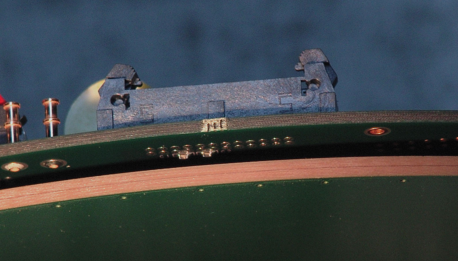
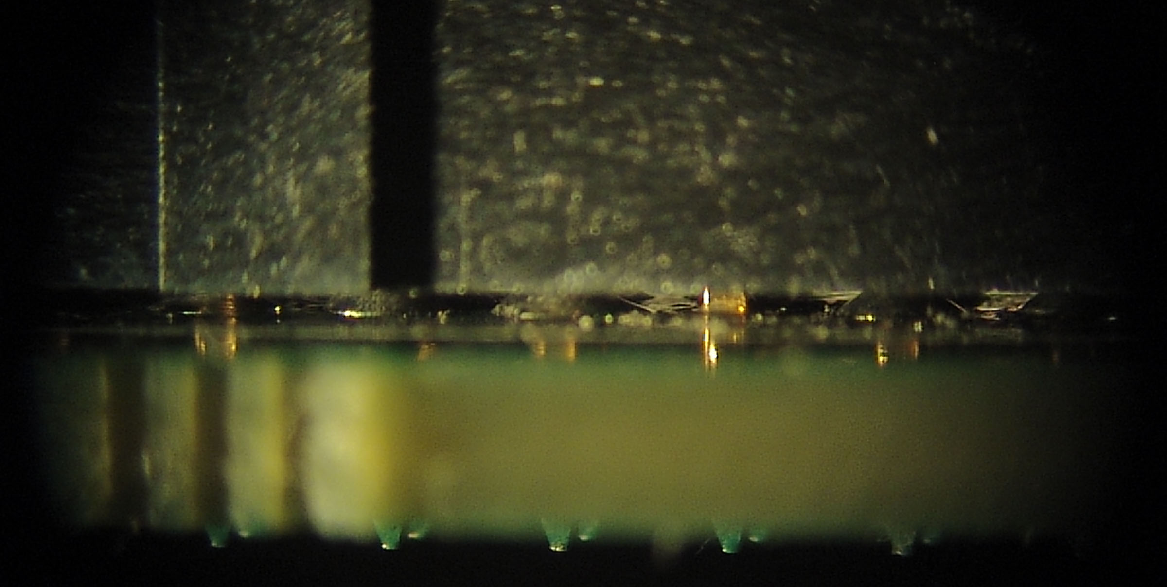
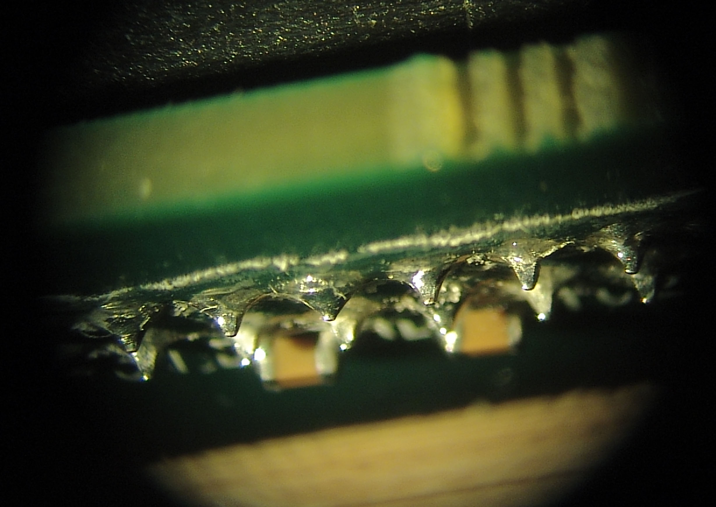
- Owing to the installation of the wrong connector onto the footprint of JP1 (the off-board HV power supply subsystem connector), a rework cycle was undertaken to mitigate the error. After rework, three PCBs (out of roughly 300) produced high-voltage power supply board test failures which were traced to shorts around JP1. Due diligence dictates that the PCBs sent to the integration sites be inspected for excessive residue from the rework process (for instance, excessive solder flux, whiskers of solder, or solder blobs or splashes that might be adhering to the PC board or flux residue).
-


-
- (these images are of a main board which was not reworked)
- (Microscope pictures do not show the residue and debris very clearly due to narrow depth of field and color shifts)


-

